Fabrication and characterisation of multi-junction phototransductors in III-V materials
Overview
- RESEARCH DIRECTION
- Gwenaëlle Hamon, Professeure - Department of Electrical and Computer Engineering
- ADMINISTRATIVE UNIT(S)
-
Faculté de génie
Département de génie électrique et de génie informatique
Institut interdisciplinaire d'innovation technologique (3IT)
- LEVEL(S)
-
2e cycle
3e cycle
Stage postdoctoral - LOCATION(S)
-
3IT - Institut interdisciplinaire d'innovation technologique
Campus de Sherbrooke
Project Description
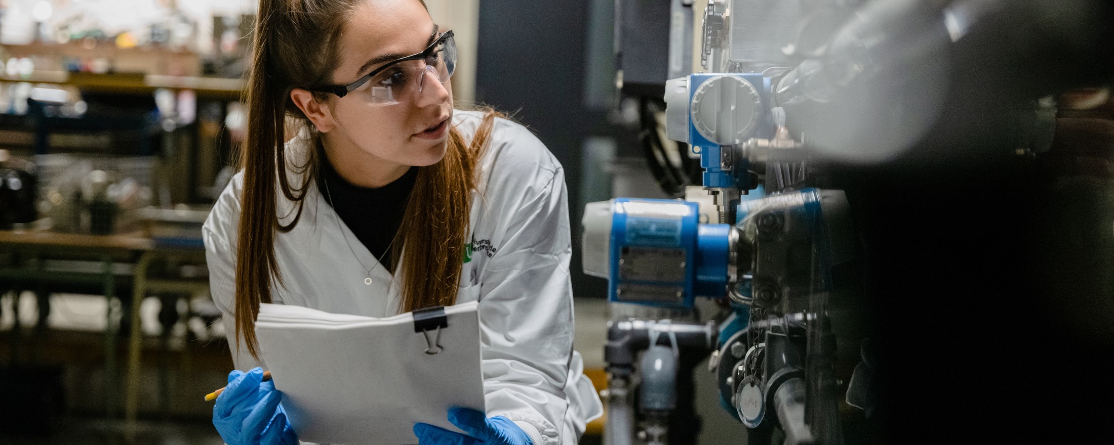
Context :
Université de Sherbrooke, and particularly the 3IT, Interdisciplinary Institute for Technological Innovation, has expertise in many cutting-edge areas of micro-nano-electronics and opto-electronics. In addition, the 3IT hosts an international joint unit of the French CNRS, Nanotechnologies and Nanosystems Laboratory (LN2), in partnership with numerous CNRS laboratories in France. The 750 m2 clean room includes numerous micro- and nano-electronics equipment, necessary for the complete manufacturing of III-V devices, in particular phototransducers, which convert mono-chromatic light into electrical power.

Subject :
Phototransducers are made from a heterostructure of III-V materials. The VEHSA structure, invented by Azastra Opto, consists of connecting several junctions in series. The manufacturing process includes plasma etching processes developed in a clean room. These cells must then be tested under laser illumination and their performance analyzed. This project, in collaboration with an industrial partner, Broadcom, would focus on the clean room manufacturing of phototransducers as well as the modeling of the electrical characteristics of cells under different conditions.
Main tasks
Manufacturing and characterization in a clean room (PECVD deposits, plasma etching, photolithography, profilometer, SEM, etc.)
Supervision and training of students on their master's and doctoral projects on the same project
Participation in project management

Required profile :
PhD, in one of the following fields: III-V materials, and/or clean room manufacturing, and/or simulation of opto-electronic components, and/or characterization of components.
Good knowledge of semiconductor physics and optoelectronics
Good methodology and analytical skills
Good interaction skills. Good working autonomy

Please send an application to Recrutement-Groupe-Hamon@USherbrooke.ca including your CV and a short text explaining your experiences relevant to the position.
We accept spontaneous applications for master's degrees, internships or doctorates.

This project can accommodate one or more students in the following programs:
- Postdoctoral fellowship
- Doctoral thesis
- Research-type master's thesis
Discipline(s) by sector
Sciences naturelles et génie
Génie électrique et génie électronique
Funding offered
Yes
The last update was on 7 May 2024. The University reserves the right to modify its projects without notice.